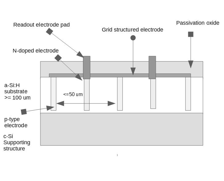
The aim of this experiment is to design, build and test a 3D detector on a hydrogenated amorphous silicon substrate (hereinafter referred to as a-Si: H). Four institutions and an industrial partner will participate in this effort: INFN-Perugia, EPFL-IMT Neuchatel, University of Wollongong (NSW-Australia) and INFN-TIFPA as research institutes and FBK Trento as industrial partner. A-Si: H is a material widely used in the construction of solar panels, so the detectors can be built at low cost and on large surfaces in production facilities for this type of devices. Another important aspect that makes this material very interesting is the intrinsic resistance to radiation; detectors made with this material can reach the level of 1015 p / cm2 without major damage and without special design techniques. A further interesting feature of this material is the possibility of be deposited, using the PECVD process, on many materials, in particular on the top of any pixel-based readout chip, avoiding expensive and problematic bonding techniques for pixel detector applications. (e.g. Bump bonding). In order to overcome the problem of the high leakage current (typical of a-Si:H) and the rather high charge collection time, we propose to construct a 3D geometry detector that allows to maintain a small collection distance (the distance between electrodes can be maintained around 20 -30 μm) having a larger detector thickness for charge generation since it is possible to grow the substrate up to about 100 μm in thickness. In this case the depletion voltage can be kept at a relatively low value of about 200 V-400 V reducing the leakage current. The radial structure of the electric field can also bring benefits on the charge collection time. This new approach, never attempted before, could improve the possibility of using a-Si: H low-cost and intrinsic resistance to radiation for the detection of MIPs.