
ARCADIA – Advanced Readout CMOS Architectures with Depleted Integrated sensor Arrays Research (2019-2021, CALL Project Proposal 2018)
Field: Detectors and Electronics
Principal Investigator: Manuel Rolo, INFN Torino
Research Units: INFN Sez. Bologna, Milano, Padova, Pavia, Perugia, Torino, TIFPA
The purpose of the ARCADIA project is to develop a novel CMOS sensor platform that allows:
- active sensor thickness in the range 50 um to 500 um or more;
- operation in full depletion with fast charge collection only by drift;
- small charge collecting electrode for optimal signal-to-noise ratio;
- scalable readout architecture with ultra-low power capability;
- easy compatibility with standard CMOS fabrication processes.
The project relies on the positive results achieved in the explorative research SEED, which led to the development of a patent-pending approach, validated on small scale sensors with an elementary readout. A strict cooperation with the silicon foundry in the context of a framework contract recently awarded by INFN through a competitive selection, will allow to further improve the sensor performance in terms of signal-to-noise ratio and power consumption. By using the latest design integration and verification methodologies, large area sensors, indispensable for a thorough validation of the concept will be deployed. A common readout framework makes it possible to characterize different sensor flavors by changing only the substrate material.
The federation of a large number of INFN units provides the critical mass and allows to foster the expertise of the national community in the field of CMOS radiation imagers, improving the competitiveness of INFN in this critical field.
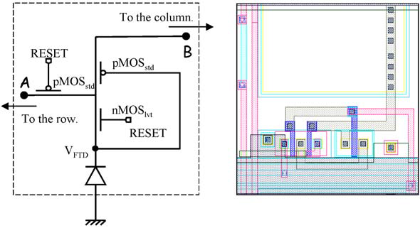
Weak Inversion Pixel Sensor (WIPS) architecture: equivalent circuit (left-hand side), corresponding layout (right-hand side).